Semiconductors devices are used in a wide range of electrical components and are susceptible to the effects of radiation. This can be a serious issue in high radiation environments such as space, especially due to the time and cost of replacing damaged components. Simulation and modeling of the radiation effects lets us understand exactly how and when the devices will fail and allows them to be designed to prevent failure.
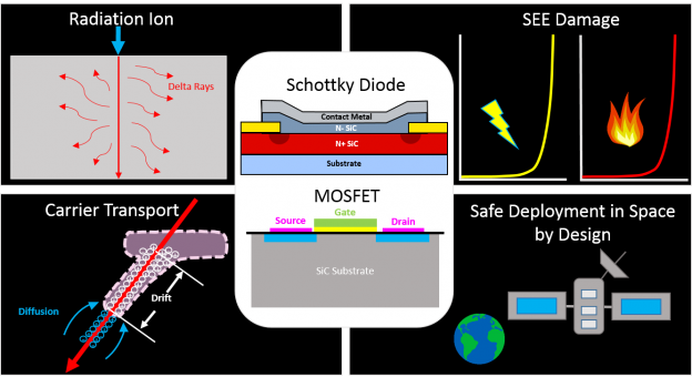
These simulations start by modeling an energetic particle colliding with the device and then moving through the semiconductor region. As the particle travels, it knocks into atoms along the way and thus deposits its energy. The energized atoms lose some of their electrons which creates an electrical current. Current is important because it will cause heating which could lead to device burnout and destruction. To perform this work, a toolkit has been developed to automate the coupling of MCNP6.2’s high fidelity radiation models with the 3D electro-thermal device simulation capabilities of Sentaurus. This facilitates realistic modeling and the design of radiation hardened devices.